
LABron Sees His Chance
Introduction
As part of this pre-lab, we were asked to lookup some useful information for the remaining portions of this lab, which will be listed out now. The largest possible memory buffer to store image information is approximately 74250 bytes. This space would be used up quite quickly usinga a standard image storage protocol like RGB565, but downsampling this to RGB332 would allow us to store double the number of pixels (in this case, 74250 pixels for a total of nearly 3 full frames in memory on the FPGA). More specific information about the hardware we're using includes:
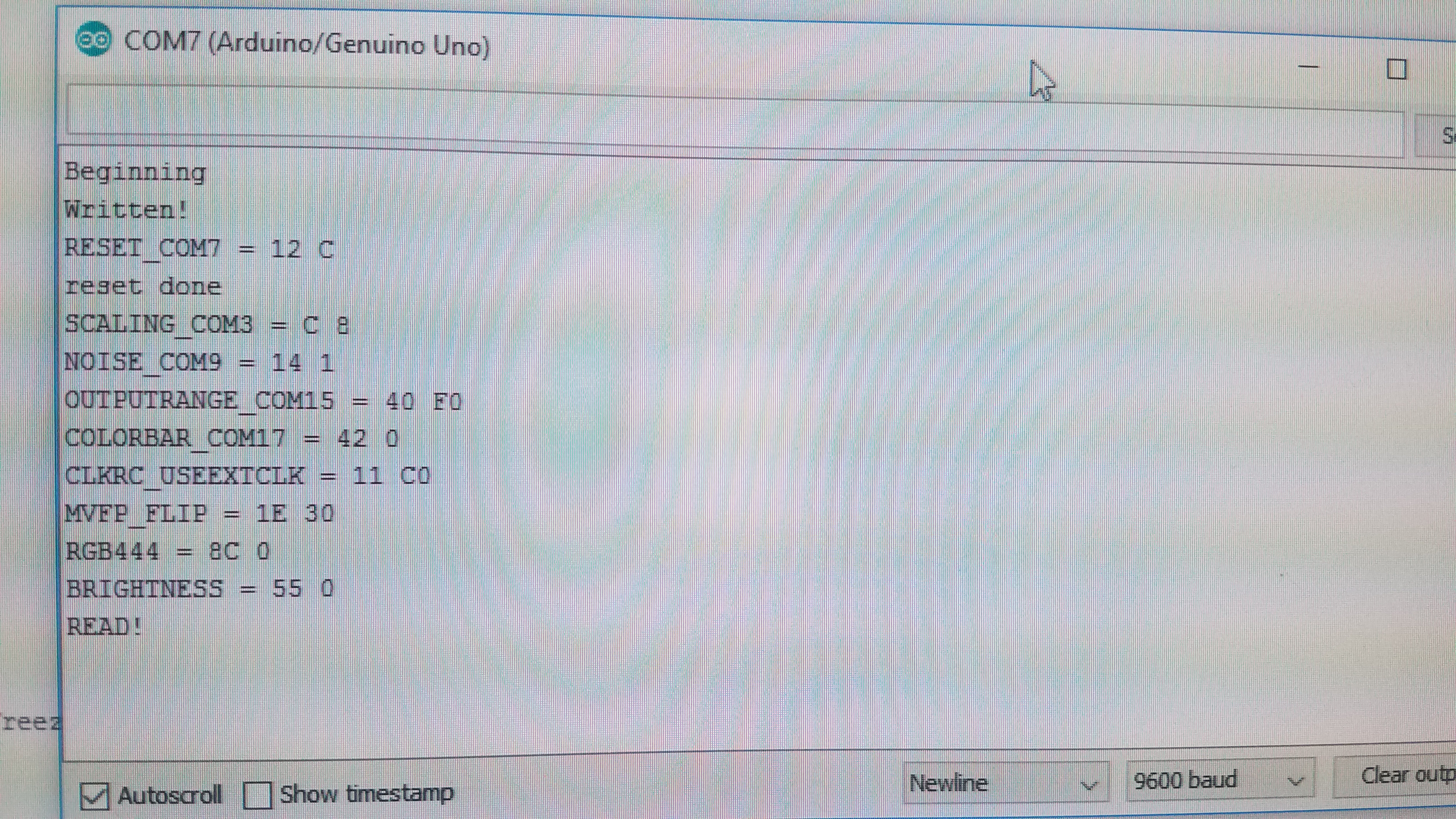
- Reg for reset: COM7 -> 0x0C
- Reg for scaling: COM3 -> 0X08
- Reg for gain control: COM9 -> 0x01 (Bit[0] froze AGC/AEC)
- Reg for external clock: CLKRC -> 0xC0 (Bit[6]: Use external clock directl)
- Reg for data formatting: COM15 -> 0XF0 (Bit[7:6]: 11: Output range: [00] to [FF]; Bit[5:4]: 11 for RGB555)
- Reg for color bar: COM17 -> 0x00 (Disable colorbar) or 0x08 (Enable Colorbar)
This wraps up the information we gathered before endeavoring on Lab 4.
Arduino Setup
One of the first things we did with our Arduino was disable the pull-up resistors on our I2C lines; this was necessary because of a voltage mismatch between the camera and Arduino (damage to the camera would results if we hadn't done this). Next, we setup our FPGA to provide a common 24 MHz clock signal to our camera and began playing around with setting registers and reading their values back on our Arduino. After this, we simply followed a camera pinout diagram and were finished with this portion of our lab.
Setting Up Our Image output
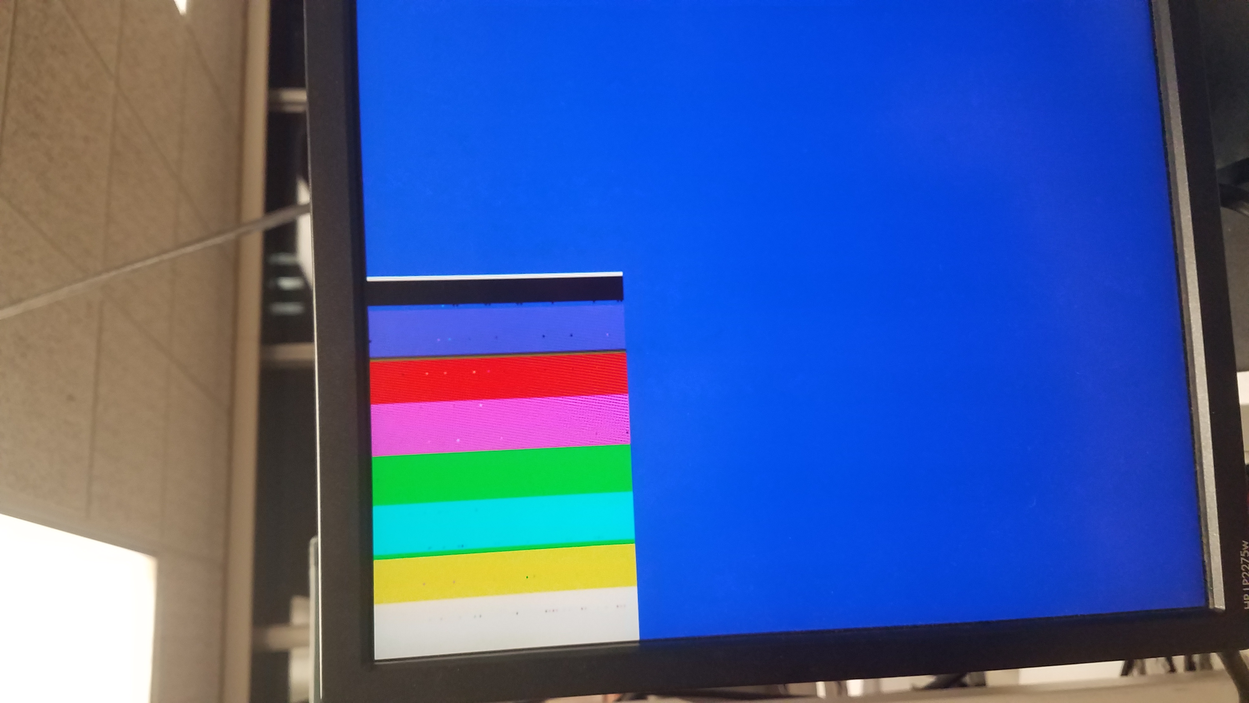
Setting up our camera involved first attaching the camera to our Arduino and FPGA, but once this was done and we were able to confirm accurate register writes, we began experimenting with reading data from the FPGA. One of the first things we did was simulate the color bars. After this, we began working with our M9K blocks and syncing up with camera frames.
Setting Up Our Camera
The most difficult part of setting up our camera was determining the order in which to check various values like VSYNC, HREF, and PCLK. However, after reading through more documentation we found the following:
- VSYNC: Determines when a new frame is starting (falling edge) and ending (rising edge).
- HREF: Determines when a new row of pixels is starting (rising edge) and ending (falling edge)
- PCLK: Determines when half of a pixel has been transmitted. New bytes start with rising edge indicates a new byte is ready to read.
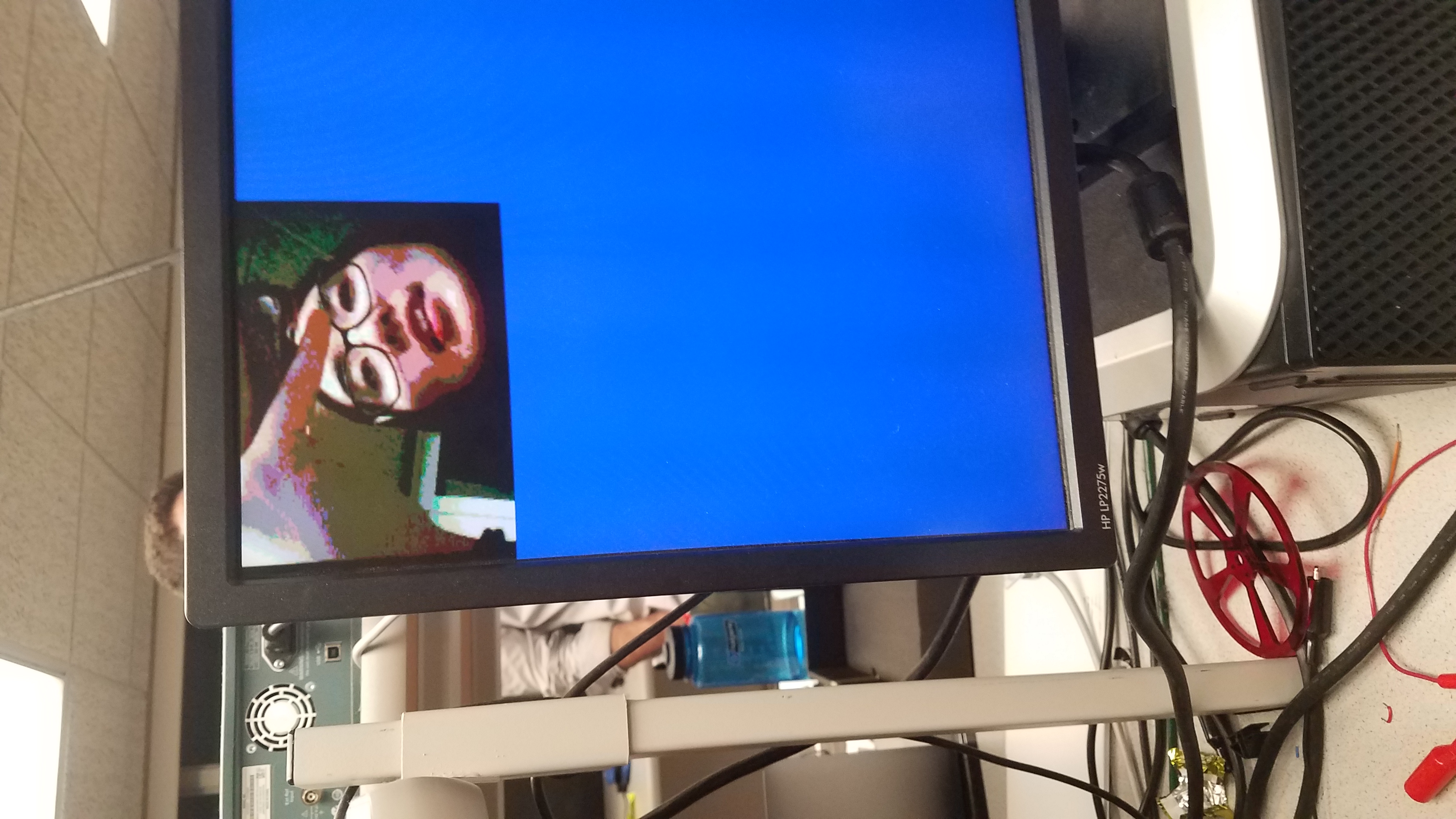
Using this information together, we were very slowly able to begin drawing full images out of our camera. Our final code was organized in a structure based around PCLK being triggered (as it switches the most often), then HREF, and finally VSYNC. This led us to finally capture the image to the left.
[Problem] Blinking Camera Image
We got the blinking image in real camera, and also discolorated color bar. We solve the blinking image based on the following concept:
- Registor: When doing downsampling, the pixel bit should directly assign to M9K memory (pixel_data_RGB332) rather than storing on a register.
- Wire: Although minimizing the wire between FPGA and Arduino is a better method, we solve the blinking image by replacing female to female with two female to male and one breadboard.
Every team has the similar problem and similar code when doing downsampling. It is better to do the sample test to test out whether the problem is from hardware or software. For example, a prestored image in M9K can be testing for image processing, or replacing certain wire to eliminate the bad wire connection.